

Inside a Semiconductor Carrier Products Factory: Hiner-pack Full Factory Tour 2026 ?
Mar 09, 2026
8 views
Chat Now
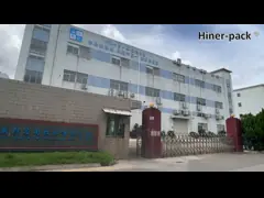
Welcome to Hiner-pack! In this comprehensive factory tour, Cathy takes you through our entire production process—from raw mold processing to the final Class 100 dust-free packaging.
As a leading one-stop supplier for semiconductor packaging/carrier, we pride ourselves on our controlled environments, automated CNC precision, and rigorous quality inspection protocols.
? Video Highlights:
0:00 Intro to Hiner-pack
0:16 Dust-Free & General Injection Molding Workshop
1:09 In-house Mold Processing & CNC Area
2:18 Quality Inspection & Reliability Test Room
3:06 Dust-Free Cleaning Workshop
3:35 Class 100 Dust-Free Packaging Workshop
4:04 EDI Ultra-Pure Water System
4:57 Conclusion
About Hiner-pack:
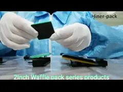
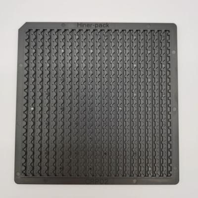
We specialize in high-cleanliness wafer shippers and semiconductor(JEDEC/IC/Chip...) trays. Our integrated approach ensures stable production and high-quality standards for global clients.
? Visit our website:
www.waferboxes.com
www.jedecictrays.com
? Inquiries:
info@hiner-pack.com
Don't forget to LIKE, SHARE, and SUBSCRIBE for more industry insights and manufacturing updates!
#Manufacturing #Semiconductor #WaferShipper #WaferBoxes #FactoryTour #Cleanroom #JEDEC #ICtrays #ChipTays #Hiner-pack
Learn More →
-
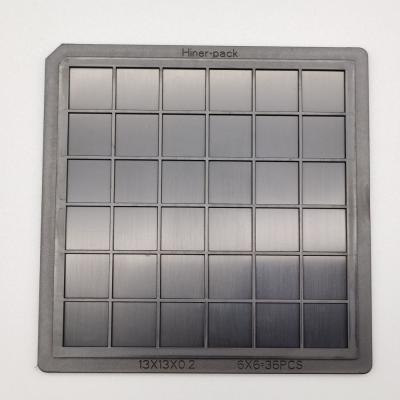
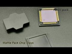
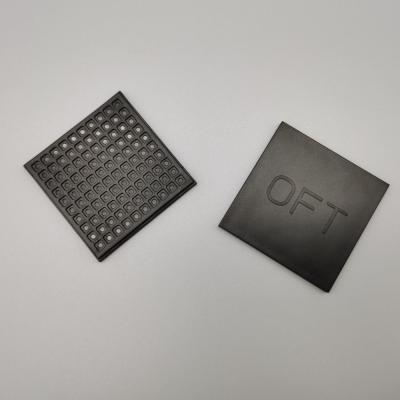
ABS MPPO Waffle Pack Bare Die Tray 36 PCS Optical Device Packaging
View Detail -

Heat Resistant Anti-Static JEDEC IC Trays Electronic Components Tray
View Detail -
Black ESD Anti Static IC Chip Tray High Temperature Resistance For Loading Sapphire
View Detail -
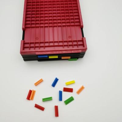
PC JEDEC IC Tray Clip 60°C-100°C Multi-Color Identification
View Detail -
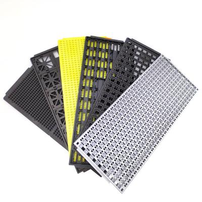
Regular Size Colorful Antistatic Shipping Trays Thermostable For IC Component
View Detail -
SGS 6/8/12 Inch Wafer Jar And Stack Box For Wafer Carrier And Storage
View Detail -
PC Waffle Pack Chip Trays For Optoelectronics Industry Loaded
View Detail