English
Sign in
| Price | negotiated |
| MOQ | 10 |
| Delivery Time | 7-15days |
| Brand | Customized |
| Place of Origin | China |
| Certification | ROHS |
| Model Number | Customized PCBA |
| Packaging Details | Standard package |
| Payment Terms | T/T, Western Union |
| Supply Ability | 10000pcs/month |
| Place of Origin | China | Packaging Details | Standard package |
| Material | FR-4, glass epoxy, FR4 High Tg | Model Number | Customized PCBA |
| Supply Ability | 10000pcs/month | Layer | 1,2,4,6,up to 22 layers |
| Certification | ROHS | Brand Name | Customized |
| Payment Terms | T/T, Western Union | Surface finish | HASL, Nickle, Imm Gold, Imm Tin, Imm Silver, OSP etc |
| PCB type | Rigid, flexible, rigid-flexible | Copper thickness | 1/2OZ 1OZ 2OZ 3OZ |
| Price | negotiated | Delivery Time | 7-15days |
| Minimum Order Quantity | 10 | name | PCB(Printed Circuit Board) Assembly |
| Stock | In Stock |
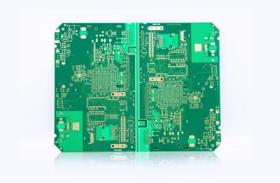
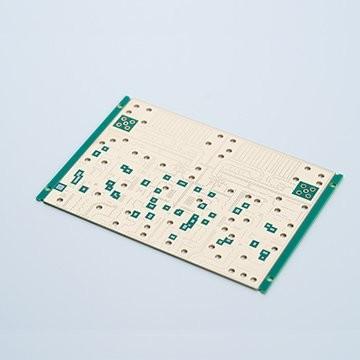
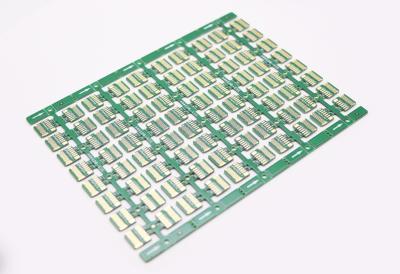
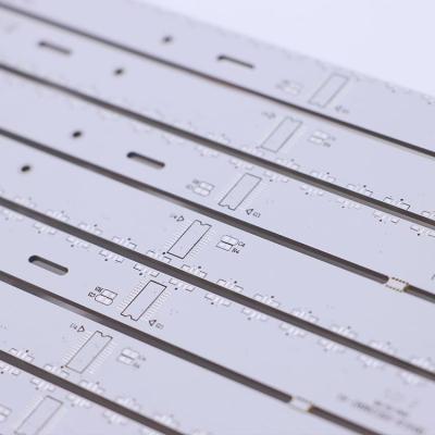
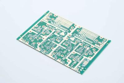
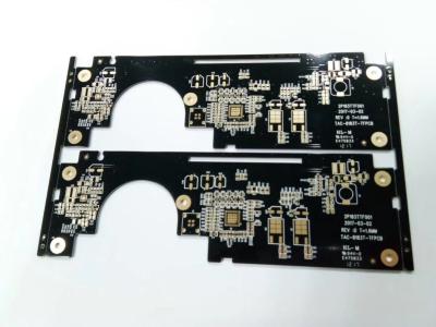
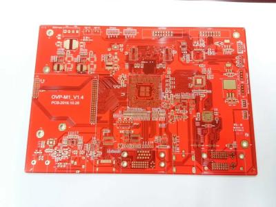
PCB(Printed Circuit Board) Assembly and SMT manufacturer one stop service
Specification
| PCB Technical Specification | |
| Order Quantity | 1-500,000 |
| Layer | 1,2,4,6,up to 22 layers |
| Material | FR-4, glass epoxy, FR4 High Tg, Rohs compliant, Aluminum, Rogers, etc |
| PCB type | Rigid, flexible, rigid-flexible |
| Shape | Any shape: Rectangular,round,slots,cutouts,complex,irregular, etc |
| Max PCB dimensions | 20inch*20inch or 500mm*500mm |
| Thickness | 0.4~4.0mm |
| Thickness tolerance | ± 10% |
| Copper thickness | 1/2OZ 1OZ 2OZ 3OZ |
| Copper thickness tolerance | ± 0.25oz |
| Surface finish | HASL, Nickle, Imm Gold, Imm Tin, Imm Silver, OSP etc |
| Solder mask | Green, red, white, yellow, blue, black, etc |
| Silk screen | White, yellow, black, or negative, etc |
| Silk screen min line width | 0.006'' or 0.15mm |
| Min drill hole diameter | 0.01'',0.25mm.or 10 mil |
| Min trace/gap | 0.075mm or 3mil |
| PCB cutting | Shear,V-score,tab-routed |
|
PCB Assembly Capabilities |
||
| Item | Technical Parameter | |
| SMT Jointing Min. Space | 0201mm | |
| QFP Space | Pitch 0.3mm | |
| Min. Package | 0201 | |
| Min. Size | 2*2 inch(50*50mm) | |
| Max. Size | 14*22 inch(350*550mm) | |
| Placement Precision | ±0.01mm | |
| Placement Precision | QFP, SOP, PLCC, BGA | |
| Placement Capability | 0805, 0603, 0402, 0201 | |
| PCB Lead time (workday(s)) Normally | |||||
| Single, Double-sided | 4 layer | 6 layer | Over 8 layer | HDI | |
| Sample Lead time (Normal) | 5-6 | 6-7 | 7-8 | 10-12 | 10-12 |
| Sample Lead time (Faster) | 48-72 hours | 5 | 6 | 6-7 | 12 |
| Mass production lead time | 7-9 | 10-12 | 13-15 | 16 | 20 |
| PCB Assembly Lead time | |||||
| Sample Lead time | PCB Fab+Components preparation +PCBA=15 workdays | ||||
| Mass production lead time | PCB Fab+Components preparation +PCBA=21workdays | ||||
Images:


Quote Requirement:
*Gerber file of the bare PCB board.
*BOM (Bill of material) for assembly.
*To short the lead time, please kindly advise us if there is any acceptable components substitution.
*Testing Guide & Test Fixtures if necessary.