English
Sign in
| Price | ≥ 5: 6 yuan/piece |
| MOQ | 1 set |
| Delivery Time | 10 Word days |
| Payment Terms | T/T |
| Supply Ability | 50000 |
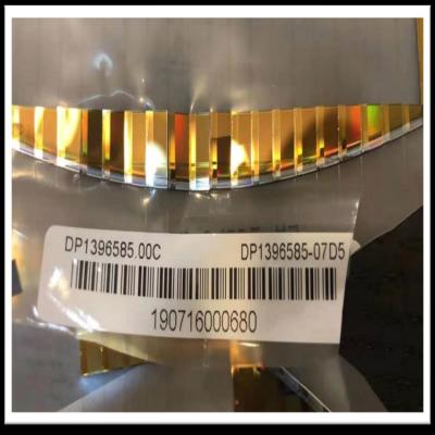
| Payment Terms | T/T | Origin | Taiwan MediaTek products |
| product name | 5nm 12" wafer scrap | memory | NANDR Flash RAM |
| application | Wafer component chip applications cover | Price | ≥ 5: 6 yuan/piece |
| Delivery Time | 10 Word days | Be applicable | smartphone car |
| Minimum Order Quantity | 1 set | Supply Ability | 50000 |
| operation | High-speed computing of AI machine system |
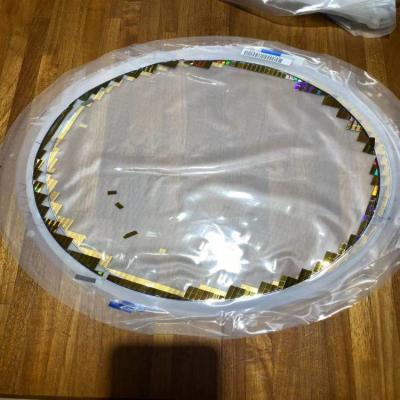
This
is
the
leftover
material
after
Jin
Yuan
is
cut,
and
the
wafer
can
also
be
taken
out.
Each
chip
can
take
about
130
wafers,
and
the
box
is
sent
by
air
in
a
box
of
three
kilograms.
It
can
also
be
shipped
in
domestic
ports.
If
necessary,
please
contact
us.
Taiwan
channel
direct
hair.

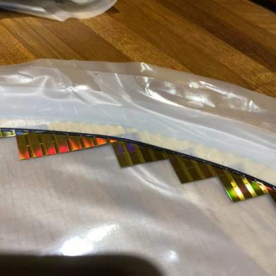
This is a subsidiary of our group for wafer and chip projects (uncut material, defective brand, finished product), and usable wafers can be removed for uncut material and defective products. Market uses are as follows:
5nm wafer 5NANO technology wafer component chip applications cover:
| 5nm wafer 5NANO technology wafer component chip applications cover: |
| ❶ Smartphone. |
| ❷AI machine system high-speed operation. |
| ❸Connect with high-end multi-party platforms such as the Internet of Things and smart cities. |
| ❹Logical calculation analysis and judgment (safety automotive IC). |
| ❺NANDR Flash random access device. Flash memory (pen drive DRAM). |
| ❻ Analog IC. Sensor. |
| ❼Microcontroller; laser cell protein medical beauty precision instrument. |
A large number of 5NANO 12” wafer processes use EUV (Extreme Ultraviolet Photolithography) technology that will continue to improve EUV’s production efficiency and yield technology. All three can be used in common.
㊀ The 12-inch 5nm chip is available in three sizes:
①.4*6m/m, ②.6*7m/m, ③.7*11m/m.
㊁The lithography line is made:
①.4*6mm is an area of 24 square millimeters, and each square millimeter has more than 177 million transistors implanted, that is, about 4.248 billion transistors, and the conversion access memory = 512MB capacity.
②.6*7mm, with a total of 7.434 billion transistors, equivalent to 1GB capacity.
③.7*11mm, there are 13.629 billion transistors in total, which is equivalent to 1.5G capacity.
Quantity: A total of 1000 boxes per month can be ordered (1.2 million pieces) / minimum order of 40 boxes (9600 pieces),
Try a box of 240 pieces. (Sample price USD 7 / PCS).
Supply period: long orders can be signed and delivered in batches
Product Specifications:
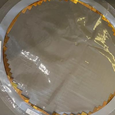
Several key points of wafer tailing processing are explained:
Global standard 12”5Nano wafer wafer, the outer periphery of each film is approximately
Size-
A
4mm
*
6mm.(About
70
to
110
chips)
Size-
B
6mm
*
7mm.(About
40
to
50
chips)
Size-
C
7mm
*
11mm.(About
16
to
24
chips)


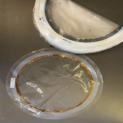
Packaged form: Including SoIC (system integrated chip), InFO (integrated fan-out packaging technology),
3DIC technology platforms such as CoWoS (Chip on Substrate Packaging), these 5nm chips are all suitable for fan in or fanout type advanced packaging technology. Although QFN, SOP, LQF, and these are all too low-end, they can all be packaged. If a lower-end packaging technology is used, it depends on the matching with the carrier board.
Package:
Carton packaging. 1kg is 80 pieces.
By air it is 3kg per box (240 pieces) By sea it is 15kg per box (1200 pieces)
The
container
is
1000
boxes
(1.2
million
pieces)
15
tons
in
weight

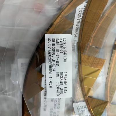
Five-nanometer wafer sample testing identifies detailed data descriptions:
The level of packaging technology requires a "five-nanometer chip" packaging factory to detect, and the packaging results are necessary and necessary to apply high-tech righteousness. "Optoelectronics Technology Professional Instrument" can detect more than 1....7E per cubic millimeter. "Transistor Structure" This instrument has 3D comprehensive functions.
Provide
test
data
in
Taiwan:

Excerpted
from
the
Internet,
for
reference
onlyIf
the
buying
volume
continues
to
exceed
the
selling
volume,
the
fund
price
on
the
The
Jiaxing
Star
Microelectronics
Co.,
Ltd.
is
affiliated
to
Jiaxing
Star
Semiconductor
Co.,
Ltd.,
which
was
established
in
April
2005.
It
is
a
company
specializing
in
the
research
and
development,
production
and
It
is
a
national
high-tech
enterprise
that
sells
services.
The
company
is
headquartered
in
Jiaxing,
Zhejiang,
with
subsidiaries
in
Shanghai
and
Europe,
and
R&D
centers
in
China
and
Europe.
It
is
currently
a
leading
enterprise
in
the
domestic
IGBT
field.
Based
on
the
past
performance
of
the
fund,
I
bought
other
fund
performances
of
these
two
fund
companies:
Galaxy
Innovation
Growth
Mix
(519674),
Cathay
Pacific
CES
Semiconductor
Chip
Industry
ETF
Link
A
(008281).
If
you
want
to
see
my
operation
of
the
A-share
technology
fund
in
real
time,
scan
the
QR
code
below
to
view
my
excellent
A-share
technology
firm
portfolio,
which
is
mainly
composed
of
semiconductor
funds
+
new
energy
funds.
In
the
end,
it's
up
to
you
to
decide
what
to
buy.