English
Sign in


| Price | USD 4.12$ per piece |
| MOQ | 100 |
| Delivery Time | 5~8 weeks |
| Brand | Cansec Wireless |
| Place of Origin | Beijing |
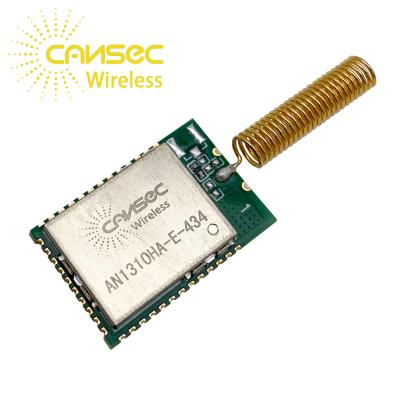
| Model Number | AN1310HA-E |
| Packaging Details | Box for 1000 pieces Package size: 40*34*20 cm Gross weight: 5.000 kg |
| Payment Terms | T/T |
| Supply Ability | 2000000 pieces per year |
| Working Frequency | 434/470/868/915MHz | RX current | 5.5mA |
| Place of Origin | Beijing | Chipset | Texas Instruments CC1310 |
| Packaging Details | Box for 1000 pieces Package size: 40*34*20 cm Gross weight: 5.000 kg | Working Voltage | 1.8~3.8V |
| RX sensitivity | -124dBm | Model Number | AN1310HA-E |
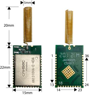
| Overall Size | 15mm*22mm (+25mm antenna)*3.2mm | Range | 400m (434MHz) / 700m (868/915MHz) |
| Supply Ability | 2000000 pieces per year | TX current | 25mA |
| Brand Name | Cansec Wireless | Payment Terms | T/T |
| TX Power | 13dBm | Price | USD 4.12$ per piece |
| Delivery Time | 5~8 weeks | Minimum Order Quantity | 100 |
| Standby current | 1uA | Antenna | Helix Connector |
Wireless RF 434 mhz Soc Ti Module 868mhz Long Range Cc1310 LoRa module

Vbat=3.3V Fquency=434/470MHz
Wireless RF 434 mhz Soc Ti Module 868mhz Long Range Cc1310 LoRa module
Features
Long-Range Mode, -110dBm at 50kbps